Future of Compute Series – AI Acceleration in Silicon
By Flavia Levi and Owen Metters, PhD
Over the last year it’s become clear that AI (artificial intelligence), is ready to change the world. But while investors, founders and policymakers alike have been gripped by the new possibilities it offers, it’s important to strike a note of caution. Beyond the ethical and existential risks AI poses (both well covered in the mainstream press), many articles have called attention to the financial and environmental costs of inference and training for LLMs like ChatGPT.
A recent article by Sally Ward-Foxton in the EE Times put this in stark terms. She estimated the hardware cost for a top-tier ChatGPT-3 training system (22k Nvidia H100 GPUs, according to the MLPerf charts) coming in at around $800m alone. The daily running cost? $700,000. It’s a wake-up call, illustrating what happens when hardware innovation struggles to keep up, and suggests that more disruptive thinking is urgently required.
For most of the history of the semiconductor industry, the brute force approach has been our best option. We packed more transistors into the same area, doubling the number every two years (per Moore’s Law). Alongside the less well-known Dennard scaling, which states that if transistor density doubles power consumption remains constant, engineers were able to squeeze more performance out of the same power and silicon area.
But in the early 2000s, both of these trends began to break down. Even the late Gordon Moore himself believed his law would reach a physical limit around 2025. It’s hard to quantify, but the growing consensus is that the computational power required to train state-of-the-art ML models has been doubling approximately every 2-3 months. It’s far more aggressive than anything predicted by Moore’s law. Even if Moore’s law does continue to apply, it might not suffice for the next big thing in AI, which could be 10x or even 100x ChatGPT’s compute requirements. Simply relying on larger data centres may not be a viable solution in the longer term.
Today, these pressures are most acutely felt by the companies developing multi-billion parameter AI/ML models. But as intelligence is pushed to the edge, we’re seeing applications that five or more years ago required dedicated GPU clusters to run are now running on laptops, or handheld devices. What is cutting edge today will be commodity tomorrow.
In the Octopus Ventures Deep Tech team, we believe this represents an opportunity for a new range of silicon-based computational paradigms. Some specialised, to implement certain techniques or models (such as AI inference), and some more generalist, addressing underlying unsolved problems in computing (such as the von Neumann bottleneck). Never, in the history of modern computing, has the drive to fix these fundamental issues been stronger.
So, what are the emerging technologies we think could unlock the compute power needed to drive the AI revolution?
Digital accelerators
GPUs were originally designed for 2D and 3D graphical generation and processing, but thanks to their ability to carry out complex mathematical operations in parallel, we’ve been able to repurpose them for use in training neural networks. This is a market now dominated by Nvidia and its CUDA platform.
But more application specific platforms have been developed. Graphcore’s IPUs, Groq’s TSPs and Google’s TPUs are all specifically designed to scale within data centres. Each aims to outcompete Nvidia. Both Graphcore and Groq reached unicorn status after impressive funding rounds, raising ~$700m and ~$350m respectively. But despite this significant funding, these companies are struggling to break Nvidia’s near-monopolistic grasp on the data centre.
Some predict that compute will continue to become more specialised, optimised for certain operations and model types. John Hennessy and David Patterson are two giants of microprocessor design. They described this phenomenon as Domain Specific Architectures in their 2018 Turing Award Lecture, highlighted again in a recent McKinsey article.) This could result in chips that are more generalisable and flexible than an ASIC, but not as general purpose and adaptable as a GPU, similar, perhaps, to an ASSP (Application Specific Standard Product). But companies in this space are moving forward cautiously, conscious of the unprecedented strides made by developers of ML models. There is a real risk that ASIC-type chips designed for today’s models may not be relevant by the time they reach market.
One of the key tailwinds in the development of more diverse, application-specific compute is the rise of RISC-V. This open-source instruction set is enabling start-ups to prototype, design and build more cheaply and efficiently, facilitating greater innovation.
Analog Computing
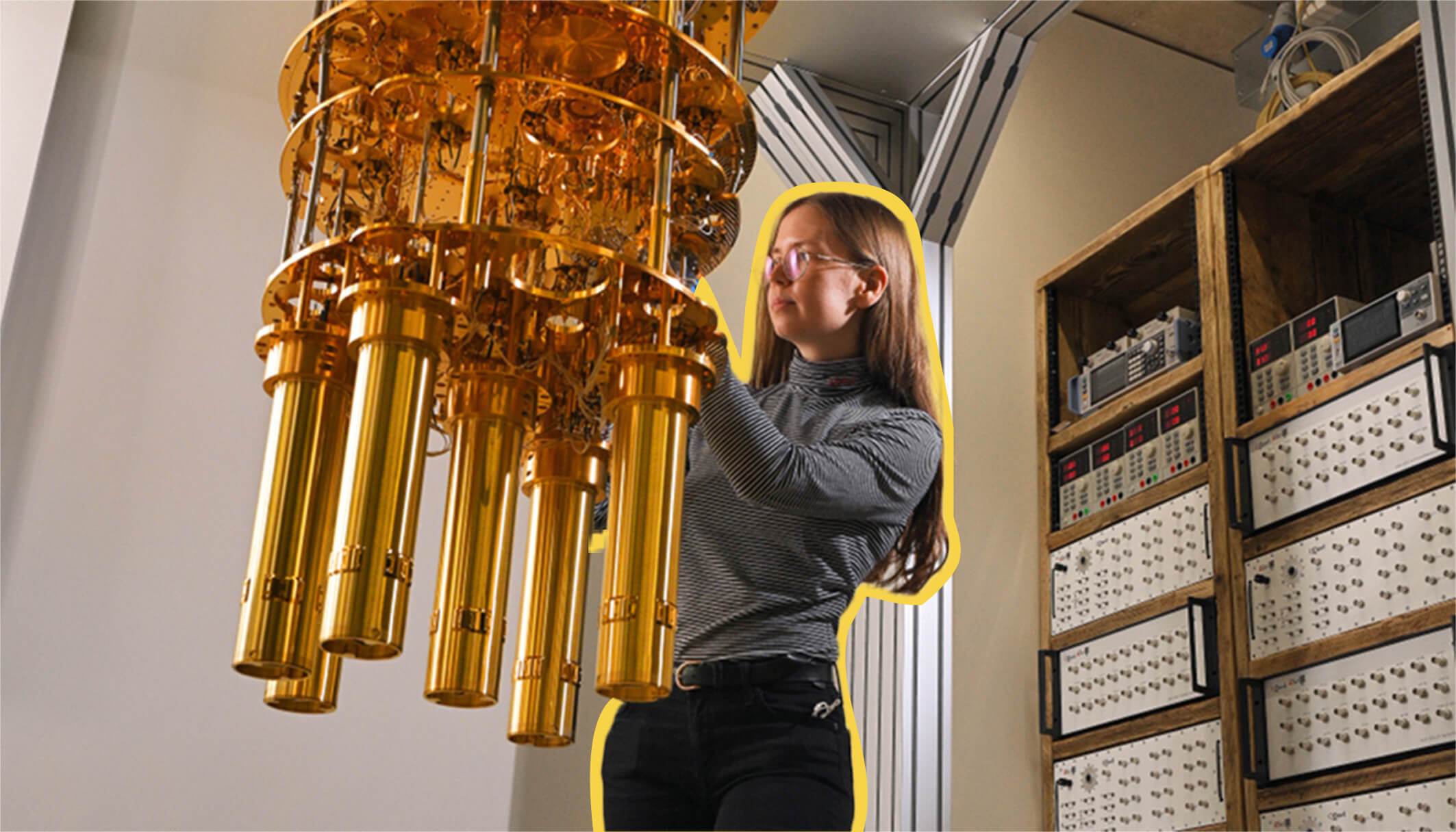
It’s possible that the issues under discussion require a more radical approach – it’s an attitude some in the field have long supported. One such approach is analog computing, something we’ve seen a real resurgence of in recent years.
Analog computing carries out manipulations on continuous range of values, not just the binary 1s or 0s used in digital systems. In a sense, they are direct implementations of the problem which is being solved. This maps on well to the matrix multiplication calculations used in neural networks, where the range of continuous values can be considered as weights in the network.
This is the principle underpinning Mythic AI’s analog “in-memory” compute chips, which repurpose flash memory cells, arranging them in a network where each cell holds a weight. These networks can be used to carry out matrix multiplications, with the “weight” held in the flash cell acting proportionally on the current flowing through it.
Analog “in-memory” computing approaches, such as those used by Mythic, can also help overcome a fundamental issue in traditional computers, or “von Neumann machines”. Von Neumann machines hold the memory and processor on separate chips, which means the processor must make calls to the memory when it requires anything stored there. When carrying out matrix multiplications as described above, for example, the processor must call the weights from the memory each time it wants to carry out a calculation. This is fine for routine tasks, but if the limits of computational speed are pushed to the max, this information transfer becomes a bottleneck and an energy sink. Analog computing, which doesn’t have this problem, could unlock far lower-energy computation.
However, due to the small variations in the fabrication of analog computing devices errors can easily propagate when dealing with variables that can take on any value within a given range. Most analog processors still need to “mark their homework” using a digital process. This analog-to-digital-and-back-again conversion can re-introduce the issue of power consumption, although proponents of the analog approach argue this is still significantly less than in classical digital systems.
Another challenge is that analog computing suffers from the lack of mature analog memory technologies, making it hard to store and update data. Still, for certain applications, where low power consumption is a priority, it’s easy to see analog devices becoming an increasingly viable option.
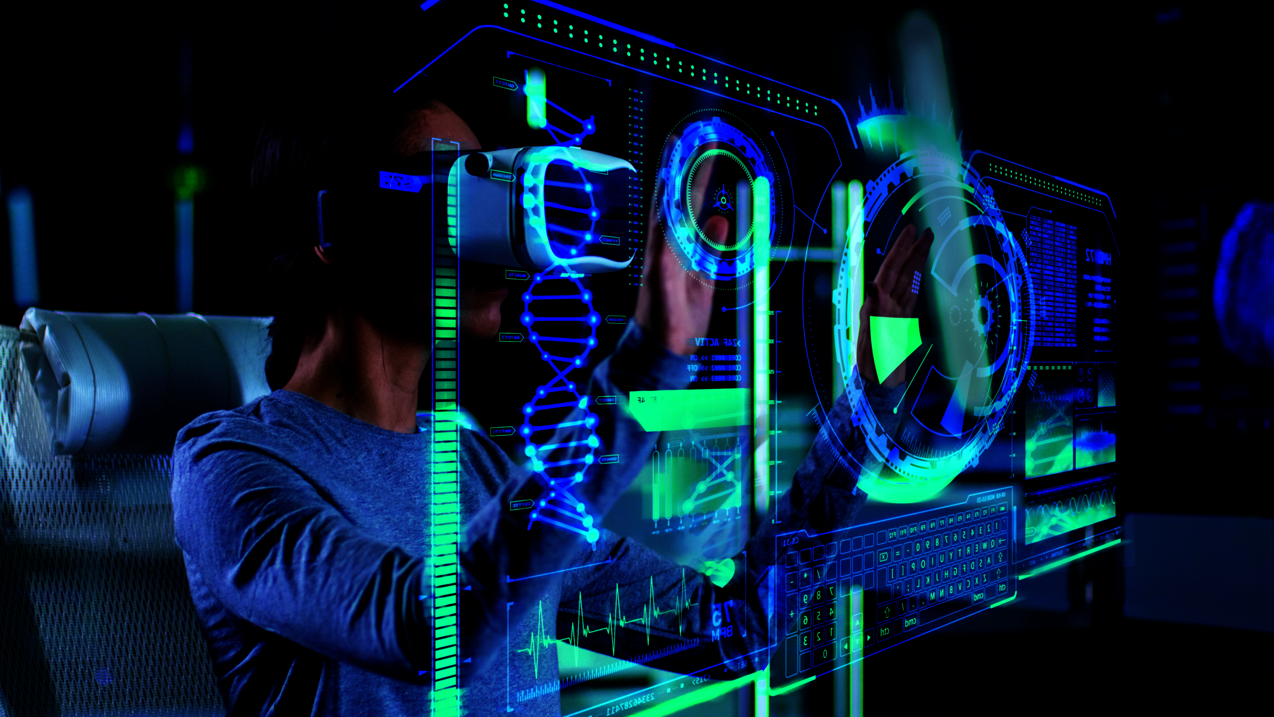
Neuromorphic Computing
Neuromorphic computing can, in some ways, be seen as a subset of both digital and analog computing and takes its inspiration from the human brain. It’s widely agreed that a neuromorphic system is characterised by the capability for in-situ learning, bypassing conventional training methodologies, as described in this paper by Dr Mehonic, CTO of Octopus Ventures portfolio company, Intrinsic.
Neuromorphic circuits can be designed using analog, digital, or mixed-mode analog/digital components. But if hardware devices are going to fully imitate the functions of synapses and neurons (e.g., building long-term memory, replicating spiking behaviour), we will likely need access to new memory technologies.
Commercially, the focus of neuromorphic chip companies has been centred on Spiking Neural Networks (SNNs). These are artificial neural networks which require stimulation beyond a threshold to trigger information transfer or computation. This “event based” processing of information means that whenever there is little or no information recorded the SNN does not fire, but when bursts of activity are detected, the SNN fires and trigger computation.
SNNs are ideally suited for processing spatio-temporal event-based information from power-efficient vision and auditory sensors (e.g., a voice activation cue like “Hey, Alexa!”). This sort of prompt would act as a “wake-up” for a more heavyweight, possibly cloud-based, compute platform. Neuromorphic chips like this offer some of the lowest power consumption per operation available, but the current applications remain relatively narrow. Still, in our rapidly evolving world of more specialised compute platforms, it’s entirely possible they will find their place.
Today, audio (e.g., noise cancellation, voice recognition, real time translation), vision (e.g., computer vision) and industrial (e.g., maintenance, monitoring) use cases dominate the edge AI market. To achieve success, start-ups in this space will need to convince customers that the economic and business advantages of shifting to novel, low-power edge AI processors outweighs the significant switching cost, in particular the requirement to rewrite existing code for a new platform.
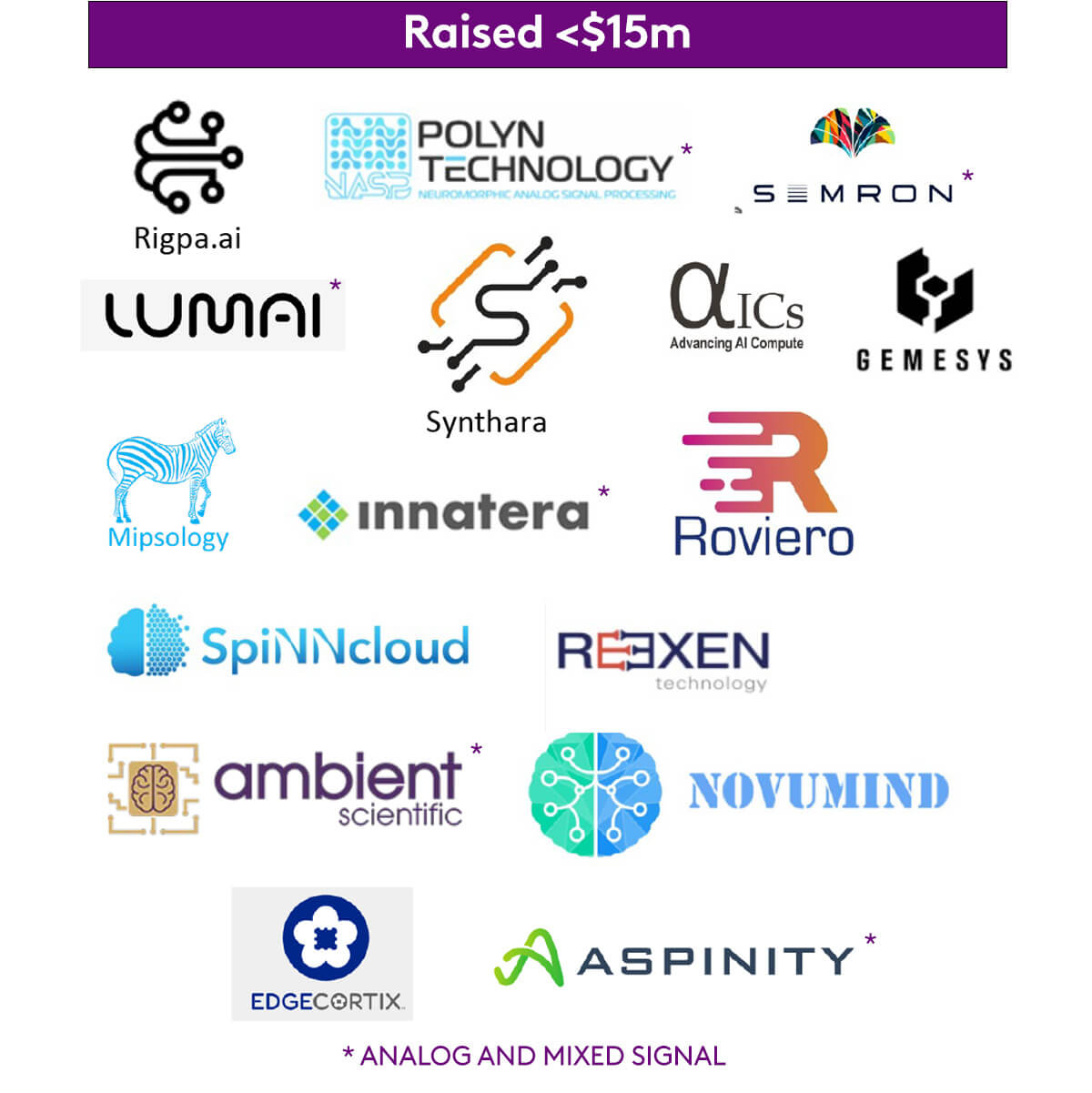
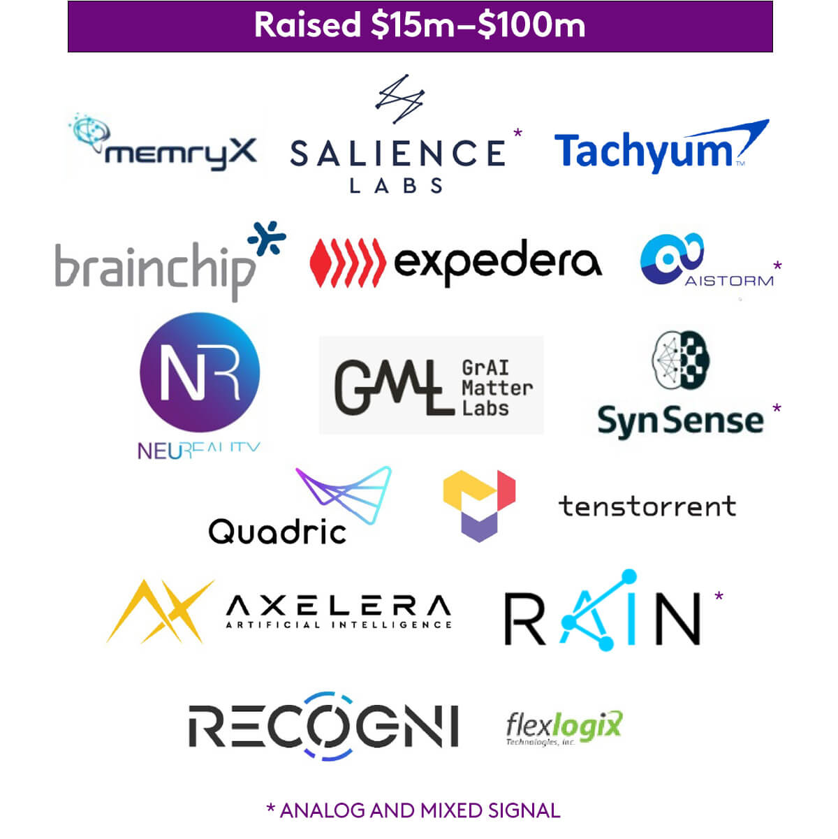
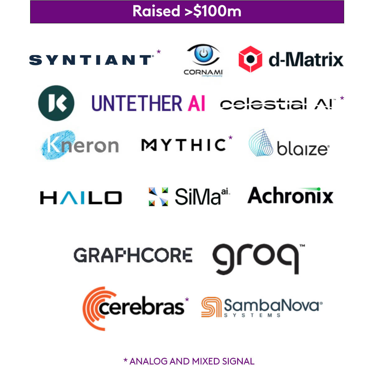
Market Mapping
We hope the market map below will offer a clear summary of the of the AI accelerator start-up landscape, from edge AI through to solutions for data centres. We’ve used data collected from Pitchbook, in addition to conversations with founders, industry, and early-backers. But given the pace at which innovation is moving in this space, we expect this to date quickly – so apologies if we have missed any information.
Conclusions and challenges
As we sum up, it’s important to highlight that this article is limited to electronic systems – we’ve chosen not to cover advances in optical or quantum computing that may yet make an impact on the trends we’ve discussed. This is because we believe that in the near term, silicon-based systems are where these problems will be solved.
Hardware accelerators continue to focus on enabling rapidly evolving ML models. The current trend is towards accelerating ever larger models in the cloud. We will likely continue to see more start-ups trying, perhaps in vain, to wrestle market share away from Nvidia spurred on by the size of the ultimate prize that a new general purpose compute platform could bring.
A key barrier to the adoption of new architectures has been the software ecosystem which accompanies them. Nvidia’s CUDA suite is an excellent example of this. Its market domination represents a sizeable blocker to any potential competitor. Newcomers, hoping to compete must not only develop better hardware – they must also convince users that their software environment is just as good, or better. This software challenge is even more apparent when looking at completely new network architectures, such as SNNs, which will require customers to adapt their models for deployment on the new hardware.
There is also a fine line for a start-up to tread between a) addressing the huge and rapidly growing market for general purpose, high-performance compute which requires significant funding and has an incredibly high barrier to entry or b) addressing a highly specific challenge where the barrier to entry is lower, but the ultimate prize may be smaller.
Our initial approach has been to invest in enabling technologies. Intrinsic is developing low-power, non-volatile memory which could be embedded into a range of processor architectures, and Codasip offers design tools and IP for companies building RISC-V processors. However, we believe there are many challenges yet to solve if AI is going to live up to its extraordinary promise. If you’re working in this space and have a world-changing solution you want to tell us about – get in touch. You can reach us at [email protected] and [email protected]
Glossary
AI inference is when the rules the AI has learned are applied in a relevant task.
ASIC (Application Specific Integrated Circuit) A chip designed for a dedicated function, rather than general use, by a specific company.
ASSP (Application Specific Standard Part) Similar to an ASIC, but marketed for multiple customers instead of a single company or organisation.
CUDA A parallel computing platform and programming model developed by Nvidia for use on GPUs.
Deep learning A type of machine learning, inspired by the human brain. It analyses data across multiple layers, allowing it to make predictions, and produce insights, with minimal human supervision.
Dennard scaling A law stating that power density remains constant as transistors shrink, so that power remains proportionate to an area.
Domain Specific Architectures A computer architecture tailored to work best within a specific application domain, rather than providing general-purpose functionality.
Edge computing Aims to improve response times and save bandwidth by storing and manipulating data closer to its source.
GPU (Graphics Processing Unit) A general purpose chip originally designed for processing graphics, but now used to train neural networks.
IPU (Intelligent Processing Unit) A new type of chip, designed by Graphcore, with the aim of processing large amounts of data more efficiently than GPUs for use in AI.
LLM (Large Language Model) A type of AI, such as OpenAI’s ChatGPT, that uses deep learning methodologies to perform language processing tasks.
Matrix A two-dimensional array of values
Matrix Multiplication A mathematical operation where two matrices are combined to generate a new matrix. This is used in neural networks to apply learned “weights” to input data resulting in an output.
ML (Machine Learning) A general term covering AI training, including deep learning, focussed on emulating human learning through the use of data and algorithms.
MLPerf (Machine Learning Performance Measurement) An independent yardstick for evaluating AI performance on key benchmarks including object detection and image classification.
Moore’s Law The rule that the number of transistors on an integrated circuit (chip) doubles about every two years.
RISC-V (Reduced Instruction Set Computer) An open-source computer architecture used to develop custom processors for a broad range of uses.
TPU (Tensor Processing Unit) An ASIC designed by Google for use in neural network machine learning.
TSP (Tensor Streaming Processor) Another chip, designed by Groq, as an alternative to the GPU for use in machine learning.
von Neumann bottleneck/von Neumann Machine Named after John von Neumann, credited with developing the theory underpinning the architecture of modern computers, a von Neumann Machine contains discrete central processing unit (CPU) and memory chips. The CPU must fetch data from the memory before carrying out an operation. These two actions cannot be carried out in parallel, which can result in a bottleneck known as the von Neumann bottleneck.